
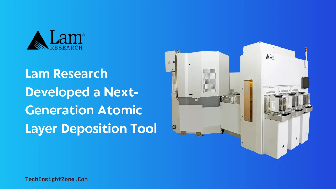
In a bold move set to redefine chip manufacturing, Lam Research Corp. has unveiled its groundbreaking ALTUS® Halo—the world’s first atomic layer deposition (ALD) tool dedicated to depositing molybdenum.
This new system is poised to replace traditional tungsten-based metallization, offering enhanced electrical performance and paving the way for next-generation memory and logic devices.
Separately, Lam Research also announced the Akara® conductor etcher, further demonstrating its commitment to advancing semiconductor technology.
However, the focus of this announcement is the revolutionary ALTUS Halo and its implications for chip scaling.
What Lam Research is Doing?

Lam Research is addressing a critical bottleneck in semiconductor manufacturing—the challenge of scaling interconnects as devices shrink.
Traditional tungsten-based metallization, while widely used, encounters limitations in ultra-thin films due to increased resistivity, which impedes performance as chip dimensions decrease.
To overcome this, Lam Research has developed the ALTUS® Halo system, a next-generation atomic layer deposition (ALD) tool that deposits molybdenum, a metal offering significantly lower resistivity.
By enabling the atom-by-atom construction of ultra-thin molybdenum layers, ALTUS Halo creates the tiny, efficient wires and connections essential for advanced semiconductors and is optimized for high-volume production.
Inside ALTUS Halo: Atom-by-Atom Deposition
So, how does ALTUS Halo achieve this breakthrough?
It harnesses the precision of ALD through a patented quad station module architecture that allows multiple processing steps to occur simultaneously—substantially boosting throughput compared to traditional single-station systems.
This innovative design is key to efficient manufacturing.
The process alternates carefully timed pulses of molybdenum precursors with precise purging steps, achieving exceptional conformality and uniformity even in high aspect ratio structures.
This meticulous, low-temperature deposition technique produces void-free, low-resistivity molybdenum layers without the need for additional barrier layers, thereby simplifying the manufacturing process while ensuring the performance and reliability required for next-generation chips.
Why Does The Innovation of ALTUS Halo Tool Matter?
1. Enhanced Electrical Performance:
Molybdenum’s lower resistivity (While bulk values may be similar, the key is the film resistivity achieved through ALD. Lam Research’s data indicates a significant reduction in resistance with molybdenum films in the ALTUS Halo system.
This translates to faster signal transmission and reduced power loss—a critical advantage as chips continue to shrink and performance demands soar. This enhanced performance could translate to faster training times for AI models, more responsive cloud services, and more powerful mobile devices.
2. Scalability for Advanced Devices:
As the semiconductor industry pushes toward increasingly miniaturized architectures, traditional tungsten metallization approaches its physical limits. Molybdenum offers a viable path to maintain device performance while enabling further scaling, allowing Moore’s Law to continue.
3. Manufacturing Consistency:
The ALD process employed by ALTUS Halo ensures uniform, high-quality film deposition. This consistency is vital for reducing defects, improving yield across production lines, and ultimately lowering manufacturing costs in high-volume fabs.
Potential Impact and Challenges

Industry experts see this development as a potential inflection point. If widely adopted, the shift from tungsten to molybdenum could revolutionize interconnect technology in semiconductor devices.
Enhanced chip performance will drive forward applications in artificial intelligence, cloud computing, and next-generation smart devices.
However, challenges remain. ALD processes, while offering atomic-level control, inherently have slow deposition rates, impacting throughput and potentially increasing manufacturing costs.
This slower rate can limit the number of wafers that can be processed in a given time, affecting overall production capacity.
Issues such as precursor stability (ensuring the precursor materials don’t degrade before they are used), high precursor wastage (minimizing the amount of precursor material that is not used in the deposition process), and integration with existing manufacturing flows (making sure the new process fits seamlessly with existing equipment and procedures) require ongoing innovation and optimization.
Instability in precursors can lead to inconsistent film quality, while integration challenges can disrupt existing production lines and increase costs.
To address the throughput challenge, researchers are exploring techniques like spatial ALD, which allows for simultaneous deposition on multiple wafers, and optimizing precursor delivery systems to increase the efficiency of the deposition process.
A New Era for Semiconductors
Lam Research’s ALTUS Halo represents not only a significant technical achievement but also a strategic response to the semiconductor industry’s evolving needs.
By introducing molybdenum into the high-volume production environment, Lam is setting the stage for a new generation of chips that are faster, more efficient, and capable of supporting the ever-increasing demands of modern applications.
Micron’s adoption of the ALTUS Halo in its NAND production further underscores the significance of this technology.
As chipmakers worldwide face mounting pressure to adhere to Moore’s Law through continuous scaling and performance improvements, innovations like ALTUS Halo offer a promising glimpse into the future of semiconductor manufacturing—a future where atomic precision meets industrial-scale production.
Also, this pursuit of enhanced chip performance is a driving force across the industry. For example, Intel’s recent advancements, presented at IEDM 2024, focus on boosting chip speed and efficiency for demanding tasks like AI.
These developments, alongside breakthroughs like Lam Research’s ALTUS Halo, demonstrate how ongoing innovation is revolutionizing semiconductor manufacturing, ensuring tomorrow’s chips can tackle the most complex computational challenges.

